Light connections
 WHAT microelectronics was to the '70s and the '80s, optoelectronics promises to be for the 21st century. Optoelectronic circuits are finding increasing use in many diverse areas like telecommunications, imaging technology and high speed computing.
One of the major areas of research has been to fabricate optical circuits. A combination of lasers, optical switches and other components on a single chip would offer tremendous advantages over conventional electronic circuits. Unlike electrons in micro-circuits, pulses of light are extremely fast and thus have the potential of improving the performance of devices several-fold. There has, however, been a minor hiccup - light cannot be easily made to bend since the optical wave-guides in use have a tendency to leak at sharp turns. This mak6 the chips large, thereby limiting their appeal (Science, Vol 268, No 5214).
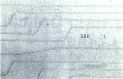
Now, Michael Krames and his group at the University of Illinois, Urbana Champaign, have built an efficient curved wave-guide (the optical equivalent of an electric wire) in a gallium arsenide-based semiconductor. Gallium arsenide semiconductors are the staple material of optoelectronics because, unlike conventional semiconductors, they emit -and absorb light easily.
To build the wave-guide, the group started with a layer of gallium arsenide sandwiched between layers of aluminium gallium arsenide. The trick is to be able to etch deep "canyons" in the material which can act as channels for the light. By masking the crystal and heating it in a controlled atmosphere, the group was able to produce a hard oxide material. This material has a lower refractive index than the original semiconductor and thus allows the light to be trapped.
The wave-guides have been found to be far more efficient than the existing ones in that the leakage losses around the bends is about 10 times less than that for the existing wave-guides. What is more, the technology is coinpatible with ordinary, existing semiconductor processing and fabrication techniques, giving it a tremendous commercial edge.
Optical chips will probably form the core of many of tomorrow's applications: whether it is terraflops optical computers or high speed switches in telecommunications. With the fabrication of the optical wave-guide, another hurdle has been overcome on this technology highway.
Related Content
- Order of the National Green Tribunal regarding forest encroachment in the process of construction of aerial ropeway connecting the base of Savitri Mandir hill to its summit in Pushkar, Rajasthan, 09/04/2025
- Mini grid solutions for underserved customers: new insights from Nigeria and India
- Land matters: can better governance and management of scarcity prevent a looming crisis in the Middle East and North Africa?
- Order of the National Green Tribunal regarding discolouration of seawater near Surathkal beach in Dakshina Kannada district, Karnataka, 18/11/2022
- African women’s report 2021: digital finance ecosystems- pathways to women’s economic empowerment in Africa
- Joint Committee report on discharge of toxic effluent generated from Sanwer Road Industrial Area, district Indore, Madhya Pradesh, 02/06/2022
